

Prepare for your exams
Study with the several resources on Docsity

Earn points to download
Earn points by helping other students or get them with a premium plan

Guidelines and tips
Prepare for your exams
Study with the several resources on Docsity
Earn points to download
Earn points by helping other students or get them with a premium plan
Community
Ask the community
Ask the community for help and clear up your study doubts
University Rankings
Discover the best universities in your country according to Docsity users
Free resources
Our save-the-student-ebooks!
Download our free guides on studying techniques, anxiety management strategies, and thesis advice from Docsity tutors
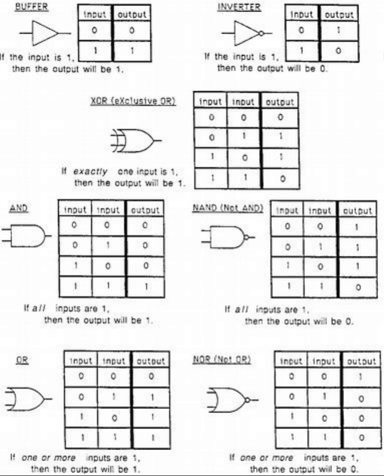
logic gate design and programming , Exams of Digital Logic Design and Programming
digital logic gate digital logic design digital circuit electronics
Typology: Exams
2016/2017
1 / 1

This page cannot be seen from the preview
Don't miss anything!